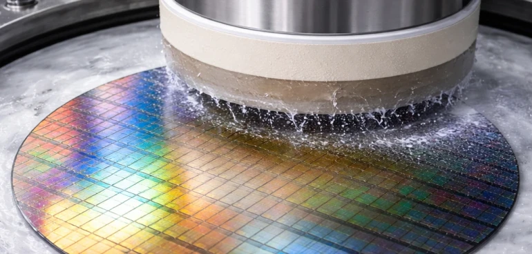

The Tactilus® wafer polishing system is engineered to reveal parallelism and pressure uniformity issues between the polishing head and wafer component.
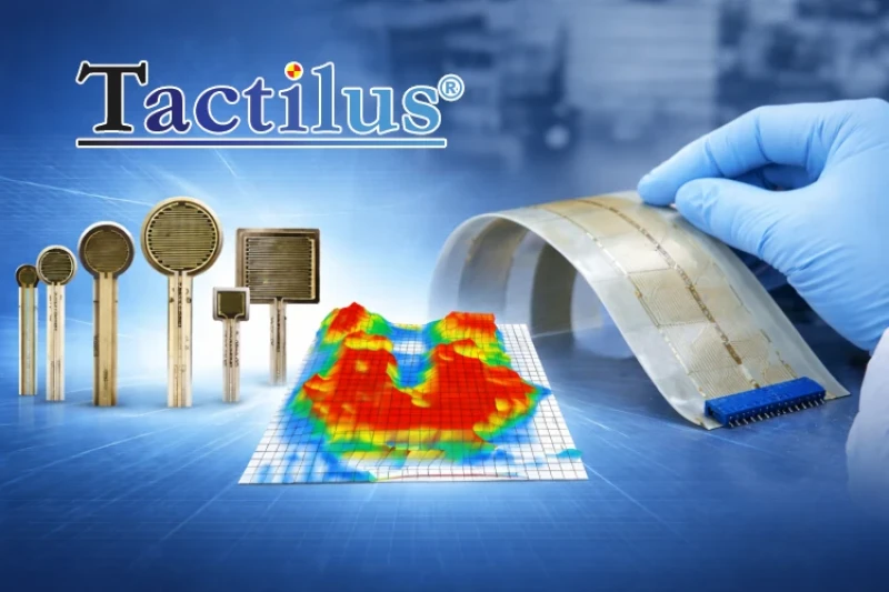
Unlike conventional pressure transducers and load cells, Tactilus® is paper-thin and designed to be placed directly on the active pressed surface, delivering unprecedented visualization of the surface pressure profile.
Tactilus® Technology
Tactilus® is a matrix-based tactile surface sensor—essentially an “electronic skin” that records and interprets pressure distribution and magnitude between any two contacting or mating surfaces.
The collected data is assimilated into a powerful Windows®-based toolkit, enabling advanced analysis and visualization. Each Tactilus® sensor is assembled to exacting tolerances, individually calibrated, and serialized to ensure precision and reliability.
Its modular architecture allows for portability, easy expansion, and simultaneous data collection from up to four discrete sensor pads.
Tactilus® employs sophisticated mathematical algorithms to intelligently separate signal from noise, along with advanced electronic shielding techniques that maximize resistance to electromagnetic noise, temperature variation, and humidity.
 Made in Italy